赤外近接場分光装置
◆装置概要
原子間力顕微鏡装置と組み合わせて、波長よりも小さい空間分解能を持つ赤外分光を行うための装置開発を行っています。
◆装置の特徴
以下の条件で装置開発中です。波数域:1000-3000 cm-1
原子間力顕微鏡:CSInstruments Nano Observer
分光は、自作のフーリエ変換分光光度計
検出器:MCT
空間分解能:200 nmを目標として開発中
◆装置アクセサリー
原子間力顕微鏡(CSInstruments Nano Observer)
◆実験・試料準備
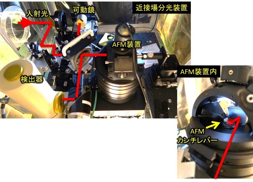
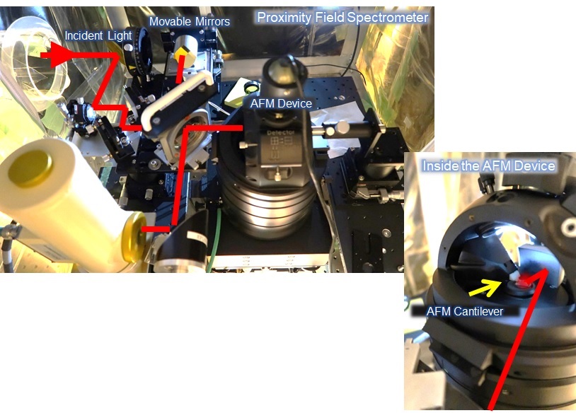
開発中の近接場分光装置は、散乱型プローブを利用する装置です。原子間力顕微鏡(AFM)装置に取り付けたプローブの先端に赤外光を集光し、散乱光の中からプローブ先端で形成された近接場光だけを抽出してスペクトルを測定します。原子間力顕微鏡と組み合わせるため、試料表面はおよそ100 nm以下で平滑である必要があります。近接場は試料表面で散乱される光であるため、100 nm程度の表面のスペクトルを反映します。したがって、試料に凹凸があり、内部の組成が異なることが期待される試料であっても、表面が均一に何らかの物質で覆われているケースでは、近接場測定では区別できない可能性があります。波数帯域が限定的であるため、この帯域にスペクトル構造を持つ試料が必要です。現状装置の問題点として、プローブ先端の散乱光のうち、試料のスペクトルを反映する近接場光を再現性良く抽出することが困難な場合があり、改良を続けています。
◆実験手順・注意事項
光学調整の手順としてまず、
平行化した赤外光を干渉計に入射し、ビームスプリッターで透過光と反射光の2方向に分割します。
分割した光の一方を可動鏡に導き、片方の光をAFMプローブ先端に集光します。
可動鏡からの反射光とプローブ先端からの散乱光を干渉させ、検出器に導きます。
AFMプローブはタッピングモードで数十KHzで振動しています。
近接場光がプローブ先端に局在していることを利用し、プローブ振動の2倍の周波数で振動している信号成分をロックインアンプで抽出します。
可動鏡の動きと信号強度を同期させて、インターフェログラムを測定し、フーリエ変換してスペクトルを得ます。
光学調整の段階では、試料としては金あるいはアルミニウムミラーを用いています。
試料位置にミラーを設置して、ロックインアンプで2次の高調波でスペクトルを確認したのちに、測定対象となる試料に設置し直します。
試料表面をAFM観察し、観測したい位置にプローグが来るように調整します。
この位置で、光を照射し、調整時と同様の手順で近接場スペクトルを測定することになります。
◆問い合わせ先
池本夕佳 このメールアドレスはスパムボットから保護されています。閲覧するにはJavaScriptを有効にする必要があります。
森脇太郎 このメールアドレスはスパムボットから保護されています。閲覧するにはJavaScriptを有効にする必要があります。
◆代表的な論文リスト
“Improvement of infrared near-field spectrum by asymmetric interferometer configuration”
Yuka Ikemoto, Michio Ishikawa, Satoru Nakashima, Hidekazu Okamura, Yuihi Haruyama, Shinji Matsui, Taro Moriwaki, and Toyohiko Kinoshita
Jpn. J. Appl. Phys. 54 (2015) 082402
10.7567/JJAP.54.082402
“Development of scattering near-field optical microspectroscopy apparatus using an infrared synchrotron radiation source”
Yuka Ikemoto, Taro Moriwaki, Toyohiko Kinoshita, Micio Ishikawa, Satoru Nakashima and Hidekazu Okamura
Opt. Comm. 285 (2012) 2212-2217
10.1016/j.optcom.2011.12.106
“Broad band infrared near-field spectroscopy at finger print region using SPring-8”
Yuka Ikemoto, Taro Moriwaki, Hidekazu Okamura, Takahiko Sasaki, Naoki Yoneyama, Atsuhi Taguchi, Yasushi Inouye, Satoshi Kawata and Toyohiko Kinoshita
Infrared Phys. Tech. 51 (2008) 417-419
10.1016/j.infrared.2007.12.016
Infrared Near-Field Spectrometer
◆Equipment overview
A new device is in development to be used for atomic force microspetrometer, which uses infrared light and has a spatial resolution smaller than the wavelength.
◆Features of the Equipment
The equipment under development have the following conditions:Wavenumber range: 1000-3000 cm-1
Atomic force microscope: CSInstruments Nano Observer
A self-made Fourier transform spectrophotometer is used for spectrometry.
Detector: MCT
Spatial Resolution: Under development with a goal of 200 nm
◆Equipment accessories
Atomic force microscope (CSInstruments Nano Observer)
◆Experiment / sample preparation
The near-field spectrometer under development is a device which uses a scattering probe. The infrared radiation is focused on the tip of a probe attached to the atomic force microscope (AFM), then the near-field light focused on the probe is extracted from the scattered light to measure the spectrum. The sample surface should be smoothed below 100 nm to be used with the atomic force microscope. Since the near-field is the light scattered off the sample surface, it reflects the surface spectrum to about 100 nm. Therefore, even if the sample is uneven, or the internal composition varies, it may not be possible to distinguish near-field measurements in the case when the surface is uniformly covered with a substance. Since the wavenumber range is limited, a sample with a spectral structure within the required range is required. A problem with the current equipment is that it is difficult to extract the near-field light that reflects the spectrum of the sample from the tip of the probe with any reproducibility, but continuous improvements are being made.
◆Experimental procedure / precautions
The first step in the optical adjustment procedure is to split the parallel infrared radiation incident on the interferometer with a beam splitter into transmitted light and reflected light.
Once the light is divided, one side is guided to the moveable mirror, and the other is focused on the tip of the AFM probe.
The light reflected from the moveable mirror, and the light scattered from the probe tip interfere with each other, and lead to the detector.
The AFM probe oscillates at tens of KHz while in the taping mode.
Utilizing the fact that the near-field light is localized at the tip of the probe, the signal components that oscillate at twice the frequency of the probe are extracted with a lock-in amplifier.
Synchronize the movement of the movable mirror with the signal intensity, then measure the interferogram and Fourier transform to obtain the spectrum.
On the optical adjustment stage, a gold or aluminum mirror are used as samples.
Install the mirror at the sample position, confirm the spectrum by the second harmonic with the lock-in amplifier, then re-install the sample to be measured.
Observe the sample surface with the AFM and adjust to the position you wish to observe.
Once the position is confirmed, irradiate the sample and measure the near-field spectrum with the same procedure as with the adjustments.
◆Contact
池本夕佳 このメールアドレスはスパムボットから保護されています。閲覧するにはJavaScriptを有効にする必要があります。
森脇太郎 このメールアドレスはスパムボットから保護されています。閲覧するにはJavaScriptを有効にする必要があります。
◆List of representative treatises
“Improvement of infrared near-field spectrum by asymmetric interferometer configuration”
Yuka Ikemoto, Michio Ishikawa, Satoru Nakashima, Hidekazu Okamura, Yuihi Haruyama, Shinji Matsui, Taro Moriwaki, and Toyohiko Kinoshita
Jpn. J. Appl. Phys. 54 (2015) 082402
10.7567/JJAP.54.082402
“Development of scattering near-field optical microspectroscopy apparatus using an infrared synchrotron radiation source”
Yuka Ikemoto, Taro Moriwaki, Toyohiko Kinoshita, Micio Ishikawa, Satoru Nakashima and Hidekazu Okamura
Opt. Comm. 285 (2012) 2212-2217
10.1016/j.optcom.2011.12.106
“Broad band infrared near-field spectroscopy at finger print region using SPring-8”
Yuka Ikemoto, Taro Moriwaki, Hidekazu Okamura, Takahiko Sasaki, Naoki Yoneyama, Atsuhi Taguchi, Yasushi Inouye, Satoshi Kawata and Toyohiko Kinoshita
Infrared Phys. Tech. 51 (2008) 417-419
10.1016/j.infrared.2007.12.016