放射光の波長を“選んで”多元合金の原子の並びを区別
~真の性能を発揮するスピンギャップレス半導体の実現へ~
2022年6月14日
高輝度光科学研究センター
大阪大学
|
高輝度光科学研究センター 田尻寛男主幹研究員、大阪大学大学院基礎工学研究科 浜屋宏平教授、名古屋大学 植田研二准教授(現早稲田大学教授)、物質・材料研究機構 桜庭裕弥グループリーダー、宝野和博フェローの研究グループは、スピントロニクス※1材料として期待されるスピンギャップレス半導体※2であるマンガン・コバルト・アルミニウム合金薄膜(三元系ホイスラー合金※3薄膜)を、3つの代表的な成膜技術を用いて作製し、大型放射光施設SPring-8※4のBL13XUを用いて、その性能と構造との関係を網羅的に評価することに成功しました。放射光の波長選択性を利用した異常分散X線回折※5などの測定から、複雑な三元系ホイスラー規則合金薄膜について、材料性能に直結する規則合金の規則性の定量化を実現しました。本研究の方法によれば、ホイスラー合金をはじめ様々な規則合金材料の設計・評価が可能となります。従来のスピンギャップレス半導体研究では物性測定が主体でしたが、同半導体に本質的な特性を実現するにはその薄膜結晶構造がきわめて重要であることを明確に示すことができ、省エネルギーな不揮発性メモリ等につながるスピンギャップレス半導体開発へ新たな指針が得られました。 【論文情報】 |
【研究の背景】
近年、スピンギャップレス半導体とよばれる新しい量子物質がスピントロニクス材料として注目されています。スピンギャップレス半導体は、磁性体であるため上向きと下向きのスピンを有するそれぞれの電子バンドが交換分裂しているのに加えて、双方のスピンバンドにエネルギーギャップを有する特殊な電子構造を持つ物質です。この特性により、例えば、電界によってその磁気特性や磁気輸送特性を変調することが可能となり、省エネルギーな不揮発性メモリ等への応用が期待されます。マンガン・コバルト・アルミニウムからなる合金は、実験的にはじめてスピンギャップレス半導体としての性質を示すことが報告された材料で、三元系ホイスラー合金でもあります。しかし、マンガン・コバルト・アルミニウム合金は非常に相分離しやすい材料で、熱力学的にも不安定であることが知られています。さらに、実際のデバイスに活用するには薄膜にする必要もありますが、その特性は、作製プロセスに大きく依存します。つまり、原子レベルの欠陥や微細構造がその特性に大きく影響していると考えられるわけですが、これまでのスピンギャップレス半導体研究では、物性測定に重きがおかれ、その特性への影響の大きさにも関わらず原子レベルの結晶構造について大きな注意は払われてきませんでした。これは、周期表で近接するマンガンとコバルトが入れ替わるなどの欠陥構造の評価は、実験室ベースのX線源では限界があるためです。
【研究内容と成果】
今回、研究グループは、マンガン・コバルト・アルミニウム合金の物性と結晶構造の関係をより深く理解するために、真空スパッタリング法、イオンビームアシストスパッタ法、分子線エピタキシー法の3つの代表的な成膜手法で同合金薄膜を作製し、物性、微細構造および、その結晶構造を詳細に調べました。このような規則合金の原子レベルの結晶構造とその欠陥構造を調べるには、放射光の波長選択性を活用した異常分散X線回折が必須でした。異常分散X線回折であれば、周期表で近接した元素であっても特定の元素に注目した解析を行うことができます(図1)。放射光実験はSPring-8のビームラインBL13XUで行われました。
得られた結果は予想外のものでした。3つの試料はすべて、これまで報告されていたスピンギャップレス半導体としての特性を満たしていましたが、微細構造および結晶構造は大きく異なっていました。真空スパッタリング法、イオンビームアシストスパッタ法では、異常分散X線回折による解析から、その結晶構造はスピンギャップレス半導体になると予測されているXA構造とよばれる結晶構造とは異なることがわかり、電子顕微鏡による観察から強く相分離していることもわかりました。分子線エピタキシー法の場合にも、単相ではなくわずかに化学組成の異なる2つの結晶相からなることがわかりました。図2に分子線エピタキシー法で成膜したマンガン・コバルト・アルミニウム合金の異常分散X線回折の実験結果と得られた結晶構造を示します。この場合もXA構造とは異なり、2相はマンガンとコバルトがお互いに入り乱れたL21B構造と乱れたL21構造であることが正確にわかりました。このように、複雑な三元系ホイスラー規則合金薄膜について、材料性能に直結する規則合金の規則性の定量化を実現しました。
このことから、過去のスピンギャップレス半導体研究では見過ごされてきた近接元素の原子規則状態を明らかにすることが、真のスピンギャップレス半導体的な電子構造を実現し、これによってもたらされる輸送特性を実用デバイスに展開するために極めて重要である、という事実が明らかとなりました。これは放射光の波長選択性を活用しなければ得られなかった成果です。
【今後の展開】
本研究の方法によれば, ホイスラー合金をはじめ新しい機能性をもつ様々な規則合金材料の設計・評価が可能となります。すなわち、異常分散X線回折により原子レベルの構造を丁寧に解析し議論していくことでスピントロニクス材料開発の指針を得ることができます。特に、SPring-8であれば実デバイスに近いナノメートル厚さの試料も評価できるため実デバイス材料への応用が加速すると期待されます。
【謝辞】
本研究は、科学研究費補助金(17H06152, 18KK0111) およびPRESTO-JST(JPMJPR17R5)の助成を受け、SPring-8の利用研究課題(2017B1313, 2018A1231, 2018B0927, 2018B1162, 2018B1538, 2018B2092)として遂行されました。

図1:スピンギャップレス半導体と異常分散X線回折の概念図。今回成膜したスピンギャップレス半導体的性質を示す合金薄膜はXA構造をとると予想されていました。しかし、走査透過電子顕微鏡像のとおり組成の近い2結晶相からなり、元素を区別できる異常分散X線回折の実験で、それらはXA構造ではなくコバルトとマンガンが入れ替わった不規則構造であることがわかりました。
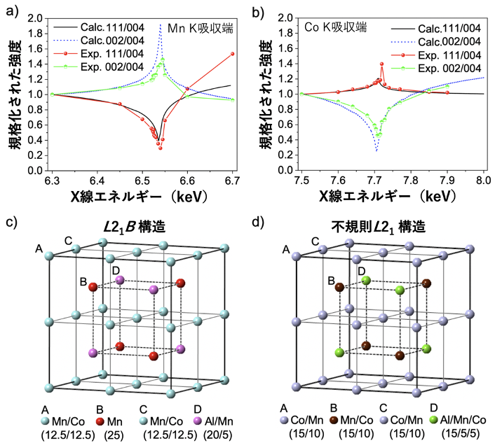
図2:異常分散X線回折の実験結果(上)と得られた結晶構造(下)
【用語解説】
※1. スピントロニクス
固体中の電子がもつ電荷と内部自由度であるスピンの両方を工学的に応用する分野のことで、スピンと電子工学をあらわすエレクトロニクスを組み合わせた造語。ハードディスクドライブのヘッドに使われている巨大磁気抵抗効果がその代表例です。
※2. スピンギャップレス半導体
固体のバンド理論において伝導電子のスピン偏極率が100%となるものをハーフメタルとよびますが、このハーフメタル性に加え半導体的性質も兼ね備えた物質をスピンギャップレス半導体とよびます。高い分極率と高移動度を併せもつため、スピントロニクスデバイス材料として注目されています。
※3. ホイスラー合金
ホイスラー合金は, X2YZの分子式をもつ典型的な規則合金で、XYZの分子式をもつハーフホイスラー合金も古くから研究されています。ホイスラー合金は1903年に非磁性の銅とマンガンとアルミニウムの3元素からなる合金が強磁性を示すことをFriedrich Heuslerが発表して以来、ハーフメタル性や磁気抵抗をはじめとして磁歪、磁気冷凍、形状記憶などさまざまな磁気効果における特異な性能の発見を通じて、スピントロニクスを含む多岐にわたる分野へと展開されています。
※4. 大型放射光施設SPring-8
兵庫県の播磨科学公園都市にある世界最高性能の放射光を生み出す大型放射光施設です。理化学研究所が所有し、利用者支援はJASRIが行っています。SPring-8の名前はSuper Photon ring-8 GeVに由来。SPring-8では、放射光を用いてナノテクノロジー、バイオテクノロジーや産業利用まで幅広い研究が行われています。
※5. 異常分散X線回折
元素には共鳴効果によって特定のエネルギーのX線に対する散乱能が大きく変化する異常分散効果が知られています。放射光のもつ波長選択性(エネルギー選択性)を活用して、このような注目元素の異常分散効果による回折強度のX 線エネルギー依存性を計測する手法を異常分散 X線回折とよびます。X線の回折現象が発見された初期の段階から日本人の貢献があり,西川正治博士が中心対称性をもたない硫化亜鉛結晶の極性判別に異常分散X線回折を利用したことはよく知られています。
|
《問い合わせ先》 |
《問い合わせ先》
田尻 寛男(タジリ ヒロオ)
高輝度光科学研究センター 散乱・イメージング推進室 主幹研究員
TEL:0791-58-0802 (内線:3443)FAX:0791-58-0830
E-mail:tajiri spring8.or.jp
桜庭 裕弥(サクラバ ユウヤ)
物質・材料研究機構 磁性・スピントロニクス材料研究拠点 グループリーダー
TEL:029-859-2708 FAX:029-859-2701
E-mail:SAKURABA.Yuyanims.go.jp
浜屋 宏平(ハマヤ コウヘイ)
大阪大学 大学院基礎工学研究科 教授
TEL:06-6850-6330 FAX:06-6850-6330
E-mail:hamaya.kohei.esosaka-u.ac.jp
植田 研二(ウエダ ケンジ)
早稲田大学 大学院情報生産システム研究科 教授
TEL:093-692-5176 FAX:093-692-5176
E-mail:k-uedawaseda.ac.jp
(報道に関すること)
高輝度光科学研究センター
利用推進部 普及情報課
TEL: 0791-58-2785 FAX: 0791-58-2786
E-mail: kouhouspring8.or.jp
大阪大学 大学院基礎工学研究科庶務係
TEL:06-6850-6131 FAX:06-6850-6477
E-mail:ki-syomuoffice.osaka-u.ac.jp
(SPring-8 / SACLAに関すること)
公益財団法人高輝度光科学研究センター
利用推進部 普及情報課
TEL:0791-58-2785
FAX:0791-58-2786
E-mail:このメールアドレスはスパムボットから保護されています。閲覧するにはJavaScriptを有効にする必要があります。
Atomic Order of Multi-Element Alloy Distinguished by “Selecting” Wavelength of Synchrotron Radiation – Bringing out the Full Performance of Spin-Gapless Semiconductors
14 June 2022
Japan Synchrotron Radiation Research Institute (JASRI)
Osaka University
|
A research group led by Hiroo Tajiri (senior scientist) of Japan Synchrotron Radiation Research Institute (JASRI), Kohei Hamaya (professor) of Osaka University Graduate School of Engineering Science, Kenji Ueda (associate professor) of Nagoya University (currently professor at Waseda University), and Yuya Sakuraba (group leader) and Kazuhiro Hono (fellow) of the National Institute for Materials Science has fabricated Mn2CoAl alloy thin films (ternary Heusler alloy*1 thin films) using three typical film growth techniques. Ternary Heusler alloy thin films are promising candidates for spin-gapless semiconductors*2 expected to be used for spintronics applications*3. This research group has comprehensively evaluated the relationship between the performance and structure of these thin films using beamline BL13XU of the large synchrotron radiation facility SPring-8*4. The degree of order in an ordered alloy is directly linked to the performance of the material. This research group has also quantified the degree of order in ternary Heusler ordered alloy thin films with a complex structure through measurements including anomalous X-ray diffraction*5, which uses the wavelength selectivity of synchrotron radiation. The technique used in this study will enable the design and evaluation of various ordered alloy materials including Heusler alloys. The conventional research on spin-gapless semiconductors has focused on property determination. However, the achievements of this study clearly indicate that information about the crystal structure of thin films is extremely important to bring out the essential characteristics of spin-gapless semiconductors. These achievements provide new guidelines for the development of spin-gapless semiconductors that can be applied to energy-saving non-volatile memories. The achievements of this study were published in Acta Materialia, an international scientific journal based in the United Kingdom, on 10 June 2022. 【Publication information】 |

Figure 1:Schematic diagrams of spin-gapless semiconductor and anomalous X-ray diffraction. It was expected that the alloy thin film with spin-gapless semiconducting characteristics grown by molecular beam epitaxy in this study would have the XA structure. However, the image from a scanning transmission electron microscope showed that the film consists of two crystalline phases of similar compositions. According to anomalous X-ray diffraction, which can distinguish between different elements, the film exhibits disordered structures in which Co and Mn are interchanged with each other instead of the XA structure.

Figure 2:Results of anomalous X-ray diffraction analysis (top) and determined crystal structures (bottom).
【Glossary】
*1. Heusler alloys
Heusler alloys are typical ordered alloys with the molecular formula X2YZ. Half-Heusler alloys with the molecular formula XYZ have also been studied for a long time. Since 1903, when Friedrich Heusler reported that an alloy composed of three elements, non-magnetic Cu, Mn, and Al, exhibits ferromagnetic properties, various unique magnetic properties of Heusler alloys have been discovered. These include half-metallic properties, the magnetoresistance effect, magnetostriction, magnetic refrigeration, and shape memory effect. Heusler alloys have been studied and applied in a wide variety of areas including spintronics.
*2. Spin-gapless semiconductors
In the band theory of solids, materials with conduction electrons that are 100% spin-polarized are called half metals. Materials having semiconductive properties in addition to half-metallic properties are called spin-gapless semiconductors. Spin-gapless semiconductors are attracting attention as materials for spintronics devices because of their high polarizability and high mobility.
*3. Spintronics
Spintronics is an area of research targeting the technological application of both the electric charges and the spins representing the internal degrees of freedom of electrons in a solid material. Spintronics was coined from “spin” and “electronics”. Currently used spintronics devices include reading heads for hard discs featuring the giant magnetoresistance effect.
*4. Large synchrotron radiation facility SPring-8
SPring-8, owned by RIKEN, is a large synchrotron radiation facility that delivers some of the most powerful synchrotron radiations in the world. It is located in Harima Science Garden City, Hyogo Prefecture, Japan. JASRI supports users of the facility. The name “SPring-8” is derived from “Super Photon ring-8 GeV”. The research conducted at SPring-8 covers a wide range of fields including nanotechnology, biotechnology, and industrial applications.
*5. Anomalous X-ray diffraction
The scattering power of elements for X-rays of certain energies varies significantly owing to the resonance effect, which is known as the anomalous dispersion effect. Anomalous X-ray diffraction is a technique of measuring the X-ray energy dependence of the diffraction intensity of target elements using the wavelength selectivity (energy selectivity) of synchrotron radiation. Japanese scientists have contributed to this area since its early stages when the phenomenon of X-ray diffraction was discovered. In a well-known study, Dr. Shoji Nishikawa used anomalous X-ray diffraction to determine the polarity of non-centrosymmetric zinc sulfide crystals.
|
《Contact》 |
《Contact》
Hiroo Tajiri
Japan Synchrotron Radiation Research Institute (JASRI)
Scattering and Imaging Division (senior scientist)
TEL:+81-791-58-0802 (ext:3443)
FAX:+81-791-58-0830
E-mail:tajiri spring8.or.jp